Passive base for Hamamatsu R5912: Difference between revisions
Create the page about Passive base and write up some rough overview of the design. The page also links to the schematic and layout files. |
Add image of amplifier module. |
||
| (One intermediate revision by the same user not shown) | |||
| Line 1: | Line 1: | ||
The Passive base for Hamamatsu R5912 is an adaptation of the current Pierre Auger Observatory base designed to work with UB/UUB and Photonis XP1805 | The Passive base for Hamamatsu R5912 photomultiplier is an adaptation of the current Pierre Auger Observatory base designed to work with UB/UUB and Photonis XP1805. It features a passive resistive divider coupled with CAEN A7501 HV power supply module. The divider is tapered on the last stages and backed by capacitors to increase linearity. Output signal can be read out from anode or amplified dynode to increase dynamic range of the readout electronics. | ||
The | The base interfaces with UB/UUB via a Canon DE-15HD power and control connector and two SMA signal connectors, one for the anode and one for the dynode output. Both signal lines are single-ended, terminated with 50 Ohms. The power/control interface consists of | ||
;+12V : Main power rail for the HV module | |||
;±3V3 : Amplifier supply rails (present only on UB) | |||
;VMON : Scaled HV monitor 0 - 5V | ;VMON : Scaled HV monitor 0 - 5V | ||
;VSET / CDE : Scaled control voltage 0 - 2.5V | ;VSET / CDE : Scaled HV control voltage 0 - 2.5V | ||
;IMON: Voltage corresponding to divider current, transimpedance 50kΩ | ;IMON: Voltage corresponding to divider current, nom. transimpedance 50kΩ | ||
; | ;TEMP±: Current loop for temperature sensor. | ||
== Prototype Base == | |||
[[File:Passive base peps.jpg|thumb|right|Passive base prototype]] | |||
The prototype base is designed to be easily modifiable to quickly test new ideas, not strictly to be optimal in cost or performance. | The prototype base is designed to be easily modifiable to quickly test new ideas, not strictly to be optimal in cost or performance. It has a E768-20B socket for the PMT and interface for the amplifier, which can be easily changed. | ||
Note that the prototype base for PEPS (SN: ''67517'') was specifically modified to work with UB. This means that the negative voltage rail converter is not populated and instead the amplifier module is powered from the ±3V3 present on the UB interface. | Note that the prototype base for PEPS (SN: ''67517'') was specifically modified to work with UB. This means that the negative voltage rail converter is not populated and instead the amplifier module is powered from the ±3V3 present on the UB interface. Original design was intended for UUB. | ||
{| class="wikitable" | {| class="wikitable" | ||
|+ DE-9 Connector Pinout | |||
! Pin # !! Signal !! Description | ! Pin # !! Signal !! Description | ||
|- | |- | ||
| Line 37: | Line 40: | ||
|} | |} | ||
=== Verification Measurements === | |||
<gallery mode="packed"> | |||
File:VsetVHV 67517.png|Vset vs. HV calibration | |||
File:VmonVHV 67517.png|Vmon vs. HV calibration | |||
File:ImonVHV 67517.png|Imon vs. HV measurement | |||
File:PSUCurrentVHV 67517.png|+12V current vs. HV | |||
</gallery> | |||
'''Design files''' | |||
*[[Media:R5912-passive-base sch.pdf|Shematic]] | *[[Media:R5912-passive-base sch.pdf|Shematic]] | ||
*[[Media:R5912-passive-base pcb.pdf|PCB Fabrication overview]] | *[[Media:R5912-passive-base pcb.pdf|PCB Fabrication overview]] | ||
=== Amplifier | Some information can also be found in the [[Media:PEPS R5912-passive-base.pdf|slides]] concerning the base. | ||
== Amplifier Module == | |||
[[File:Amplifier-module-peps.jpg|thumb|right|Amplifier module prototype]] | |||
In the original Auger base design, the amplifier takes the signal from the last dynode and amplifies it with gain of about 45 V/V (33 dB) to achieve dynode/anode ratio of 32 (the amplified signal from the dynode is 32x signal from the anode). Bandwidth should be at least 30 MHz, larger than the 20 MHz anti-aliasing filter in the UB frontend. | |||
The prototype amplifier module is also based on the Auger design, built around the AD8012 dual-channel current feedback amplifier. The amplification is split into two stages with a high-pass filter in between to remove any offset voltage. | |||
=== Verification Measurements === | |||
<gallery mode="packed"> | |||
File:Module peps magnitude.png|Magnitude vs. frequency (sinewave) | |||
</gallery> | |||
'''Design files''' | |||
*[[Media:Opamp-prototype sch.pdf|Schematic]] | *[[Media:Opamp-prototype sch.pdf|Schematic]] | ||
*[[Media:Opamp-prototype pcb.pdf|PCB Fabrication overview]] | *[[Media:Opamp-prototype pcb.pdf|PCB Fabrication overview]] | ||
| Line 49: | Line 75: | ||
---- | ---- | ||
If you encounter any problems, don't hesitate to contact me | If you encounter any problems, please don't hesitate to contact me [mailto:havelka@fzu.cz]. | ||
Latest revision as of 13:51, 28 July 2026
The Passive base for Hamamatsu R5912 photomultiplier is an adaptation of the current Pierre Auger Observatory base designed to work with UB/UUB and Photonis XP1805. It features a passive resistive divider coupled with CAEN A7501 HV power supply module. The divider is tapered on the last stages and backed by capacitors to increase linearity. Output signal can be read out from anode or amplified dynode to increase dynamic range of the readout electronics.
The base interfaces with UB/UUB via a Canon DE-15HD power and control connector and two SMA signal connectors, one for the anode and one for the dynode output. Both signal lines are single-ended, terminated with 50 Ohms. The power/control interface consists of
- +12V
- Main power rail for the HV module
- ±3V3
- Amplifier supply rails (present only on UB)
- VMON
- Scaled HV monitor 0 - 5V
- VSET / CDE
- Scaled HV control voltage 0 - 2.5V
- IMON
- Voltage corresponding to divider current, nom. transimpedance 50kΩ
- TEMP±
- Current loop for temperature sensor.
Prototype Base

The prototype base is designed to be easily modifiable to quickly test new ideas, not strictly to be optimal in cost or performance. It has a E768-20B socket for the PMT and interface for the amplifier, which can be easily changed.
Note that the prototype base for PEPS (SN: 67517) was specifically modified to work with UB. This means that the negative voltage rail converter is not populated and instead the amplifier module is powered from the ±3V3 present on the UB interface. Original design was intended for UUB.
| Pin # | Signal | Description |
|---|---|---|
| 1 | NC | No connection |
| 2 | IMON | Divider current monitor |
| 3 | VMON | Voltage monitor 0 - 5V |
| 4 | VSET | Voltage control 0 - 2.5V |
| 5 | +12V | Power rail |
| 6 | +3V3 | Positive opamp rail |
| 7 | -3V3 | Negative opamp rail |
| 8 | GND | Ground |
| 9 | GND | Ground |
Verification Measurements
-
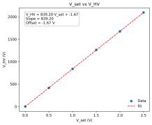 Vset vs. HV calibration
-
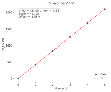 Vmon vs. HV calibration
-
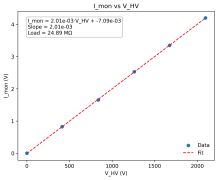 Imon vs. HV measurement
-
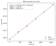 +12V current vs. HV


Design files
Some information can also be found in the slides concerning the base.
Amplifier Module

In the original Auger base design, the amplifier takes the signal from the last dynode and amplifies it with gain of about 45 V/V (33 dB) to achieve dynode/anode ratio of 32 (the amplified signal from the dynode is 32x signal from the anode). Bandwidth should be at least 30 MHz, larger than the 20 MHz anti-aliasing filter in the UB frontend.
The prototype amplifier module is also based on the Auger design, built around the AD8012 dual-channel current feedback amplifier. The amplification is split into two stages with a high-pass filter in between to remove any offset voltage.
Verification Measurements
-
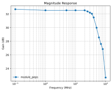 Magnitude vs. frequency (sinewave)

Design files
If you encounter any problems, please don't hesitate to contact me [1].
